Hey, you know, in the fast-changing world of telecom, RF Bias networks are kind of a big deal. When you start digging into how these systems work—especially with stuff likeDistributed Antenna Systems (DAS) and Base Transceiver Stations (BTS)—it really hits home that understanding their design and how to use them properly is key to keeping our networks running smoothly. HiLinks Technology Co., Ltd., a pretty innovative tech company based in Shenzhen since 2008, has been right there at the cutting edge, focusing on super advanced RF products that help boost network performance and reliability.

This 2025 guideis here to give you a solid, easy-to-understand overview of RF Bias networks. We'll cover their main parts, what you need to think about when designing them, and how they’re practically used. Thanks to our years of experience and a bunch of industry awards, HiLinks is dedicated to helping engineers and designers get the most out of these networks. As folks keep demanding better, more reliable communication systems, really understanding how theseRF Bias networks tick is going to be more important than ever if you want your systems to perform at their best.
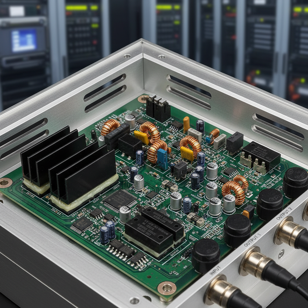
RF Bias networks play a crucial role inradio frequency (RF) designs by facilitating the proper operating conditions of active components such as transistors and amplifiers. These networks are composed of resistors, capacitors, and inductors that determine the DC bias point while allowing RF signals to pass through. By understanding the key components and their functions, engineers can optimize performance and ensure stability in RF devices.
Tips:When designing an RF Bias network, always consider thefrequency response of your components. Using high-quality components minimizes loss and distortion, which is critical at RF frequencies. It’s also essential to simulate the network under various conditions to identify potential issues before prototyping.
Another vital aspect is the layout of the bias network. Proper grounding and minimizing trace lengths can significantly impact performance. Pay attention to impedance matching between the bias network and the RF component to avoid reflections that can degrade signal quality. Employing test points in your layout will simplify troubleshooting and help refine the design further.
Effective design principles are crucial when implementing RF Bias networks in various applications, especially in advanced systems like Distributed Antenna Systems (DAS) and Base Transceiver Station (BTS) systems. Properly designed RF Bias networks ensure optimal performance and reliability by providing stable DC power to active components while isolating them from unwanted RF signals. Factors such as impedance matching, thermal management, and filtering must be taken into consideration to prevent signal distortion and maintain efficiency.
Tips for designing effective RF Bias networks include using high-quality components that can withstand the specific operational environment and ensuring that the layout minimizes parasitic effects. Additionally, it's important to conduct thorough testing in realistic conditions to assess the network’s performance across a range of frequencies.
At HiLinks Technology Co., Ltd., our extensive experience in RF product design empowers us to address the unique challenges associated with RF Bias networks. By leveraging innovative technologies and adhering to rigorous design principles, we consistently deliver reliable and high-performance solutions tailored to meet the demands of the telecommunication industry.
In the realm of radio frequency (RF) design, selecting the right components for bias network configurations is crucial for optimal performance. According to a recent report by MarketsandMarkets, the global RF components market is expected to reach $30.0 billion by 2025, driven by increasing demand for efficient communication systems. This underscores the paramount importance of understanding the intricacies of RF Bias networks, which serve as pivotal elements in maintaining consistent operating conditions for active devices.
To achieve the desired functionality of an RF Bias network, it is essential to choose components that not only meet the electrical specifications but also align with operational reliability. Key components include resistors, capacitors, and inductors which must be selected based on their thermal stability and frequency response. A report by IEEE indicates that low-noise amplifiers and mixers are particularly sensitive to biasing conditions, reinforcing the need for precision in component selection. By carefully evaluating the characteristics of these components, designers can ensure compliance with stringent performance standards while significantly enhancing the overall system efficiency in diverse applications such as telecommunications and radar systems.
| Component Type | Typical Value | Frequency Range (GHz) | Power Rating (W) | Application |
|---|---|---|---|---|
| Resistor | 50 Ω | 1 - 10 | 0.5 | Impedance Matching |
| Capacitor | 10 pF | 0.5 - 6 | 0.25 | Biasing and Filtering |
| Inductor | 1 μH | 1 - 10 | 0.3 | DC Blocking |
| Diode | 1N4148 | 0.1 - 5 | 0.5 | Switching |
| Transistor | BJT | 0.1 - 10 | 1 | Amplification |
In RF bias network design, engineers often encounter several common challenges that can impact both the performance and reliability of wireless systems. One significant issue is achieving consistent impedance matching across various frequencies. According to a 2022 industry report by the International Journal of RF and Microwave Computer-Aided Engineering, mismatched impedances can lead to a 20-30% decrease in power efficiency, which is particularly critical in applications requiring high linearity. Addressing this requires careful selection of components and strategic layout considerations to ensure seamless integration within the overall RF architecture.
Another challenge lies in managing thermal stability and noise figure, particularly in high-frequency applications. A study from the IEEE Transactions on Microwave Theory and Techniques highlights that inadequate bias stabilization can increase sensitivity to noise, degrading signal integrity. Implementing robust thermal management solutions and employing advanced bias techniques, such as temperature-compensating resistors, can significantly reduce these effects. By focusing on these common challenges, designers can enhance the performance of RF bias networks, ensuring they meet the stringent demands of modern communication systems.
When it comes to optimizing RF bias networks, understanding the specific application scenarios is crucial for achieving peak performance. For instance, in wireless communication systems, maintaining consistent bias levels across varying environmental conditions ensures that the transceiver operates efficiently. Designers must consider elements like temperature fluctuations and operational frequencies, which can significantly affect the reliability of bias networks. This requires a combination of careful component selection and layout strategies that minimize parasitic elements, thereby enhancing signal integrity.
In environments such as satellite communication, where signal quality is paramount, the bias network must be robust against interference and noise. Employing filtering techniques and impedance matching can help maintain optimal performance under these challenging conditions. Additionally, incorporating adaptive biasing techniques can provide dynamic compensation for shifts in performance, ensuring that the network continues to operate reliably over its lifespan. These tailored approaches not only enhance system resilience but also enable engineers to meet the increasing demands of .
Testing and validation techniques play a crucial role in the development and deployment of RF bias networks. These methodologies ensure that the designed networks function effectively under varying conditions and meet performance specifications. Utilizing a systematic approach, engineers can employ simulation tools to model the RF bias networks before physical prototyping. This process involves iterative testing to examine the response of the network under different frequencies, power levels, and environmental factors, which is essential for refining designs.
Moreover, the integration of advanced techniques such as machine learning (ML) can significantly enhance the validation process. Techniques like cross-validation, employed in various fields including medical diagnostics and environmental monitoring, ensure that the data used for validating RF bias networks is robust and reliable. By reshuffling data samples and testing multiple subsets during each iteration, practitioners can derive insights that improve the accuracy of their predictions regarding network performance. As RF technology continues to evolve, the incorporation of such modern validation strategies will be vital for achieving optimal results in RF bias network design and application.
This chart illustrates the distribution of different testing and validation techniques used in RF bias networks as of 2025. The focus is on ensuring optimal performance and reliability in various applications.
: RF bias networks provide stable DC power to active components while isolating them from unwanted RF signals, ensuring optimal performance and reliability in applications like Distributed Antenna Systems (DAS) and Base Transceiver Stations (BTS).
Key factors include impedance matching, thermal management, and filtering to prevent signal distortion and maintain efficiency.
Using high-quality components that can withstand the operational environment minimizes the risk of failures and ensures reliable performance.
A well-planned layout helps to minimize parasitic effects, which can distort signals and negatively impact network efficiency.
They ensure that RF bias networks function effectively under varying conditions and meet performance specifications through systematic approaches and iterative testing.
Engineers use simulation tools to model networks before physical prototyping, allowing them to examine responses to different frequencies, power levels, and environmental factors.
Machine learning techniques, such as cross-validation, enhance the robustness and reliability of validation data, improving the accuracy of performance predictions.
HiLinks Technology leverages extensive experience and innovative technologies to meet the unique challenges of RF bias networks, focusing on delivering high-performance solutions for the telecommunication industry.
Iterative testing allows for the refinement of designs by repeatedly examining the network's performance under various conditions, ensuring reliability and effectiveness.
The integration of modern validation strategies, like machine learning, is essential as RF technology evolves, playing a vital role in achieving optimal design and application results.
The article "2025 Guide to RF Bias Networks: Understanding Design and Application" provides a comprehensive overview of RF bias networks, highlighting their key components, functions, and design principles essential for effective implementation. It emphasizes the importance of selecting appropriate components for various RF bias network configurations and addresses common challenges faced in the design process, offering practical solutions. Additionally, the article explores application scenarios that optimize RF bias networks for enhanced performance and discusses testing and validation techniques to ensure reliability.
HiLinks Technology Co., Ltd., with its extensive experience since 2008 in designing advanced RF products for Distributed Antenna Systems (DAS) and Base Transceiver Station (BTS) systems, is well-positioned to leverage the insights provided in this guide. The company's commitment to innovation aligns with the principles outlined in the article, ensuring robust and efficient RF bias network solutions for their clients.